 |
| Current state. |
In addition to progress work on the PCB, it appears like the direct port writing for the software is working just fine. In dealing with software, I need to put some more time into figuring out the timers to correctly change states on the PIC on the chipKIT.
 |
| Beginning Layout. |
 |
| Design 1. |
The photo to the right is the first design of the PCB. However, this seems to occupy too much space, so this design was abandoned.
 |
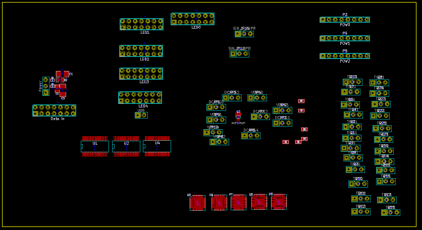
| Explanation. |
The PCB in it's current design. It seems to occupy less space than before. Now to explain all of the parts of it:
1. Power circuit. Includes filtering capacitors, and at this point has 5V for the logic levels, a 5V high-amperage line for driving the transistors, and a 3.3V for the logic levels on the TLC5940s.
2. Jumpers to select what mode the 5940's are in. +'s are denoted for positive side of jumpers.
3. Data in and Serial Jumpers. These are configured for either the first or second board in a line-up.
4. TLC5940's and gnd side of the LEDs. This is where the magic for PWM happens for a given LED. We are planning on using more of the 14 pin ribbon cable connecting layers back to the master board to connect between the ground side of the LEDs and this panel PCB.
5. This is the power side for a line of LEDs. This uses the demuxes to select which of 24 transistors to drive a row of LEDs on the cube. Each row requires about 1.5 A; hence, high amperage traces are used.
Pink Lines:
These will have either ribbon cable headers or direct solder connections for a given panel. These will be connected to a given square of LEDs. The solder connections were used on the power side because a panel's PCB does not need to be removed easily.
Yellow lines:
The only external connections that a panel's PCB has to the outside world. It features a 14 pin ribbon cable connector for all of the data. If you have been paying attention, each panel only requires 12 data lines, the extra 2 are used to select which PCB in a 2 layer chain this board is. That is what the jumpers located in Box #3 above is used to select. There is also a power connection in the upper-right hand corner of the PCB that has a common ground, 5V logic, and 5V high amperage line.
Hopefully in the next day or 2 I should be able to finish out the PCB design.
PCBs Components are mounted on a non-conductive board and connected with small pathways, called "traces." Because they are usually designed on a computer, printed circuit boards fit many components in a minimum amount of space. They replace the much larger wires used in the past. Thanks a lot.
ReplyDeletePrototype PCB Assembly Services